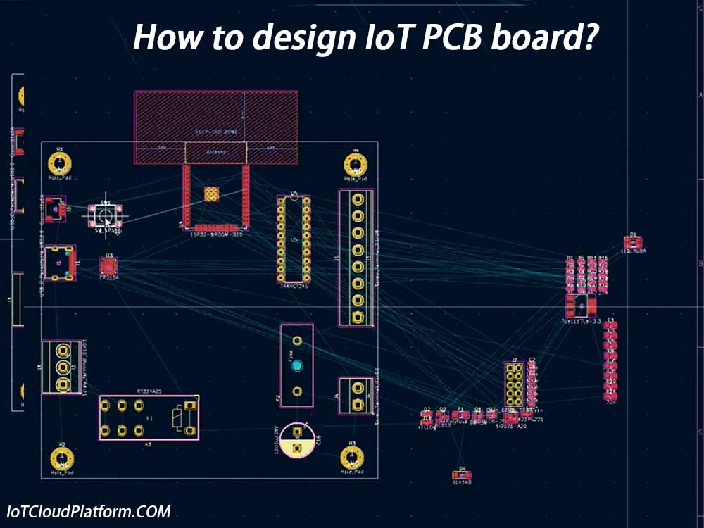
How to design IoT PCB board?
Designing Internet of Things (IoT) PCB boards is a complex and meticulous process that involves multiple considerations, including preliminary preparation, PCB structure design, layout and routing, rule setting, inspection and optimization, production and board making, and other steps.
Preliminary preparation
Determine design requirements
- Functional requirements: Clarify the functions that IoT devices need to implement, such as data acquisition, transmission, processing, etc.
- Environmental adaptability: Consider the environment in which the device will be deployed, such as temperature, humidity, electromagnetic interference, etc., to select appropriate materials and processes.
- Cost budget: Determine the number of layers, materials, components, etc. of the PCB board based on the project budget.
Prepare design materials
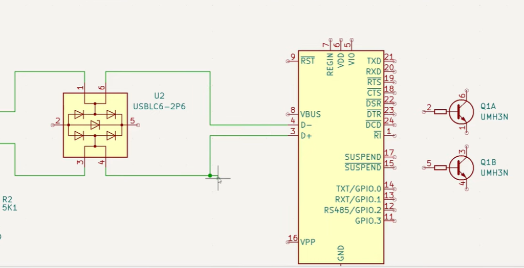
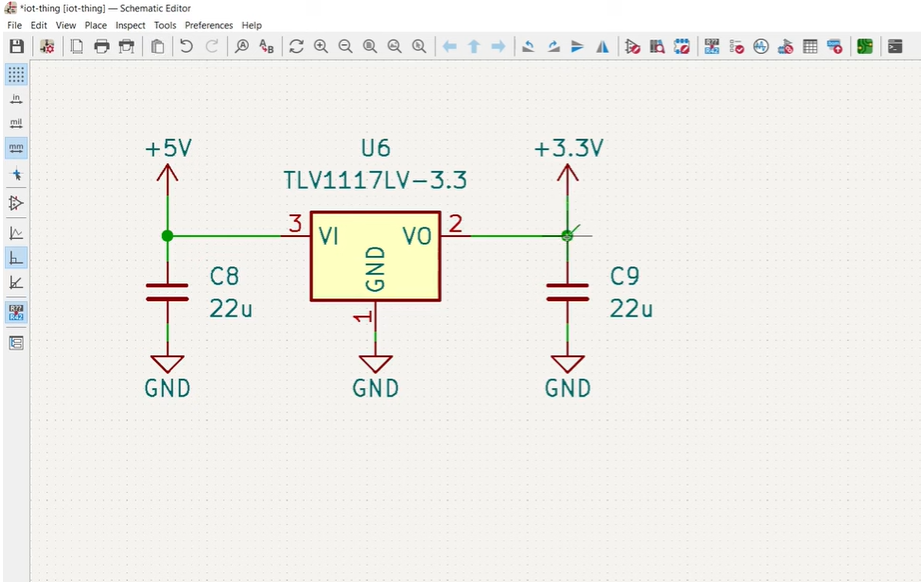
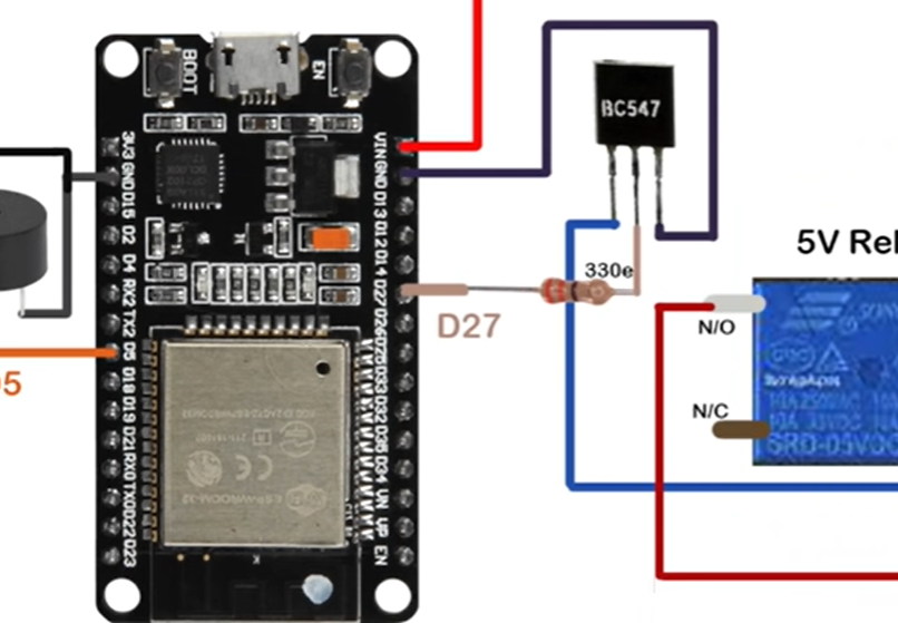
- Schematic diagram: Draw a circuit schematic diagram to clarify the connection relationship between the components.
- Package library: Create or prepare a PCB package library based on the standard size information of the selected components. The package library directly affects the installation of the board and requires special attention.
- Product definition book: Contains detailed specifications, performance indicators, etc. of the product as the basis for design.
PCB structure design
Board shape design
- Shape matching: Design the shape and size of the PCB board according to the product appearance and internal structure.
- Positioning form: Use the boss and positioning ribs to jointly position to ensure the accurate position of the PCB board in the device.
- Component layout: According to the number and size of components, rationally plan the layout of components on the PCB board.
Detail consideration
- Space reservation: Reserve enough space for subsequent structural design and component installation.
- Cut-out processing: Cut-out the edge of the PCB where side keys or other fixed structures need to be installed.
- Thickness selection: The thickness of the PCB board is generally 1.0mm. If there are fewer components and circuits, a thinner thickness can be selected.
Layout and wiring
PCB layout
- Electrical performance partitioning: Divide the PCB board into digital circuit area, analog circuit area, power drive area, etc. to reduce mutual interference.
- Functional block layout: Circuits that complete the same function should be placed as close as possible, and the components should be adjusted to ensure the simplest connection.
- Heat dissipation consideration: Heat-generating components should be placed separately from temperature-sensitive components, and thermal convection measures should be taken if necessary.
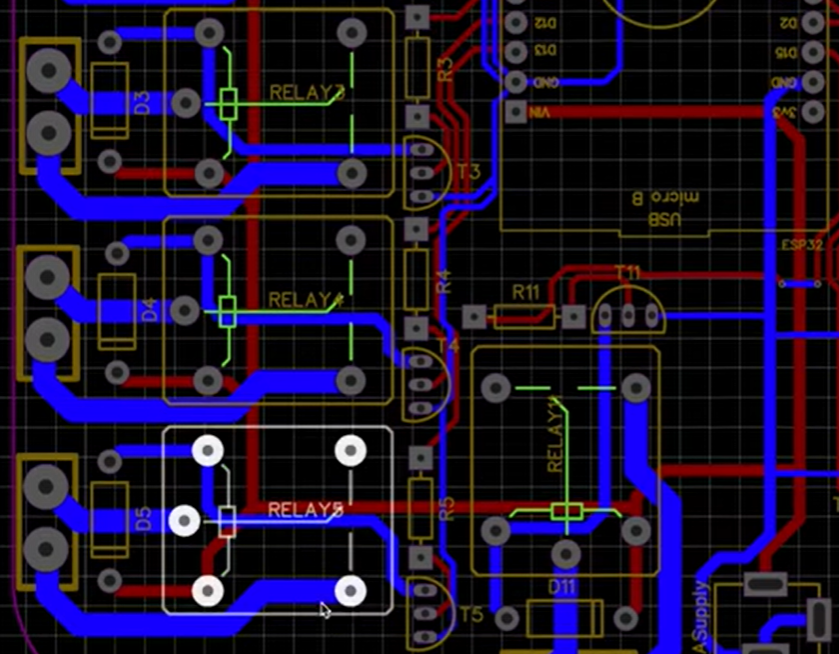
PCB wiring
- Power line and ground line wiring: First, the power line and ground line should be wired to ensure the electrical performance of the circuit board. Try to widen the power and ground line widths, and the ground line width should be larger than the power line width.
- Signal line wiring: When wiring, pay attention to the direction and spacing of the signal line to avoid reflection interference and parasitic coupling.
- Wiring optimization: On the basis of wiring through the line, optimize the wiring to improve the electrical performance and aesthetics of the circuit board.
Rule setting
- Line width and line spacing: Set reasonable line width and line spacing according to the importance and frequency of the signal. Generally, the signal line width is 0.2~0.3mm, and the power line width is 1.2~2.5mm.
- Pads and vias: Set the size and spacing of pads and vias to ensure the installation and welding quality of components.
- DRC check: Use the DRC (Design Rule Check) tool to check whether there are any violations of the rules in the PCB design, such as insufficient line width, too small spacing, etc.
Check and optimize
Network and DRC check
- Network check: Ensure that all components and networks are connected correctly.
- DRC check: Use the DRC check tool to find and fix problems in the design.
Structural check
- Interference check: Check whether there is interference between the PCB board and the device housing and other components.
- Space utilization: Optimize the layout and wiring of components on the PCB board to improve space utilization.
Output and production
Output photolithography file
- Convert PCB design files to photolithography files for PCB board production.
PCB board production
- Engineering EQ confirmation: PCB board factory engineers confirm the photolithography files to ensure that they meet production requirements.
- Board production: According to the photolithography files, PCB board production is carried out.
SMT and testing
- SMT data output: Prepare SMT data, including component position numbers, coordinates and other information.
- SMT and welding: Mount components on the PCB board according to the SMT data and weld them.
- Testing and debugging: Test and debug the welded PCB board to ensure normal function.
Summary and archiving
- Summarize design experience: Summarize the lessons learned in the design process and provide reference for subsequent projects.
- Technical file archiving: Archive and save technical files such as design data, schematics, PCB design files, and test reports for future reference and reuse.
Special considerations and advanced technologies
Electromagnetic compatibility (EMC) design
EMC is a very important aspect in IoT PCB design. Improper design may cause interference between devices, affecting the stability and reliability of the system. Therefore, when laying out the wiring, the following aspects need to be specially considered:
- Power supply filtering: Add appropriate filtering circuits to the power input to reduce interference from the power supply.
- Ground design: Use a star-shaped ground layout to reduce ground loops and reduce common-mode interference.
- Signal integrity: Pay attention to the termination matching of high-speed signal lines to reduce reflection and radiation.
- Shielding design: For sensitive circuits or high-frequency circuits, consider using a metal shielding cover for isolation.
Thermal management
IoT devices often need to operate under various environmental conditions, including high-temperature environments. Therefore, thermal management is also an important aspect of PCB design. Here are some thermal management strategies:
- Reasonable layout: Disperse components with high heat generation to avoid heat concentration.
- Use heat sink: Install heat sinks on heat-generating components to increase the heat dissipation area.
- Ventilation design: Design ventilation holes on the device casing to use convection to dissipate heat.
- Thermistor isolation: Isolate temperature-sensitive components from heating components to prevent overheating damage.
Reliability and durability
IoT devices usually need to run stably for a long time, so the reliability and durability of PCB design are also very important. Here are some ways to improve reliability and durability:
- Select high-quality components: Select components that have been strictly screened and tested to ensure reliable quality.
- Strengthen solder joint connection: Use large pads and thick lines to enhance the load-bearing capacity and reliability of solder joints.
- Redundant design: Use redundant design in key circuit parts to improve the fault tolerance of the system.
- Aging test: Perform aging tests during the product development stage to simulate environmental conditions for long-term operation, identify potential problems and solve them in a timely manner.
Design and production collaboration
In the process of IoT PCB design, the collaboration between design and production is crucial. Designers need to maintain close communication with PCB board manufacturers, component suppliers, etc. to ensure the feasibility of the design plan and the efficiency of production. Here are some key points for collaborative work:
- Process capability assessment: In the early stage of design, communicate with the PCB board factory to confirm its process capability to ensure the feasibility of the design plan.
- Production file confirmation: Before production, confirm the accuracy and completeness of the production files (such as photolithography files) with the PCB board factory.
- Sample testing and feedback: Obtain samples and test them in time during the production process, and feedback the test results to the design team and PCB board factory so that problems can be found and improved in time.
- Mass production preparation: After the sample test is passed, coordinate the preparations for mass production with the PCB board factory and component suppliers to ensure smooth production.
Future trends and new technologies
With the continuous development of IoT technology, PCB design is also evolving. Here are some possible future development trends and new technologies:
- Flexible PCB (FPC): Flexible PCB has the advantages of light weight, small size, and bendability, and has broad application prospects in wearable devices, smart medical and other fields.
- High-density interconnect (HDI) technology: HDI technology achieves higher-density line connections through microvias, blind vias, and buried vias, which helps to achieve smaller and higher-performance IoT devices.
- Three-dimensional packaging technology: Three-dimensional packaging technology achieves more compact packaging and higher integration by stacking multiple chips or components, which helps to improve the performance and reliability of IoT devices.
- Artificial intelligence-assisted design (AI-CAD): With the development of artificial intelligence technology, AI-CAD will become an important trend in the field of PCB design. Through technical means such as machine learning and big data analysis, AI-CAD can automatically complete some design tasks and improve design efficiency and accuracy.
In summary, IoT PCB design is a complex and meticulous process that requires comprehensive consideration of multiple factors.
Through continuous learning and practice, designers can continuously improve their design level and contribute to the development of the IoT industry.
FAQs about IoT PCB
There are many factors to consider when choosing the right PCB board, including mechanical strength, electrical performance, heat resistance, chemical resistance, cost, etc. Common boards include FR-4 (glass fiber epoxy resin), CEM-1 (paper-based epoxy resin), metal-based boards, etc. FR-4 has become the first choice for most IoT PCB boards due to its good electrical properties and processing performance.
Layout and routing are important links in PCB design. The layout should follow the principle of “big first, small later, difficult first, easy later”, that is, important unit circuits and core components should be laid out first. When routing, signal integrity should be considered, key signal lines (such as high-speed signals, clock signals, etc.) should be arranged first, and the signal path should be shortened as much as possible to reduce bends and vias. In addition, attention should be paid to the layout of power lines and ground lines to reduce electromagnetic interference.
Signal integrity is an issue that needs special attention in IoT PCB design. To ensure signal integrity, differential signal transmission, increasing signal line spacing, selecting appropriate transmission line types (such as microstrip lines, strip lines, etc.), and impedance matching can be used. At the same time, attention should be paid to the distribution of power and ground to avoid problems such as voltage drop and ground bounce.
The design of the power supply system needs to consider factors such as voltage stability, current demand, and conversion efficiency. In IoT PCB boards, switching power supplies or linear regulators are often used as power supply solutions. When designing, it is necessary to reasonably plan the power and ground planes, and use a multi-layer board structure to distribute the power and ground to different levels to reduce cross-interference. In addition, decoupling capacitors need to be placed at key circuit nodes to filter out high-frequency noise and improve power supply stability.
Thermal design is an important measure to prevent components from overheating, performance degradation, and shortened life. When designing, components with high heat generation need to be dispersed to avoid local heat concentration. At the same time, boards and heat sinks with high thermal conductivity can be used to improve heat dissipation efficiency. When possible, add heat dissipation holes or fans and other heat dissipation channels to further improve the heat dissipation effect.
Design for manufacturability (DFM) is the key to ensuring that circuit boards can be produced smoothly. When designing, it is necessary to follow the PCB design specifications and the manufacturer’s requirements to ensure the manufacturability of the design. For example, it is necessary to reasonably set process parameters such as trace width, trace spacing, and aperture; avoid using overly complex layouts and wiring methods; choose standard components instead of custom components, etc. In addition, potential problems in the production process need to be considered in the design stage and avoided in advance.
Testing and verification are important links to ensure the performance and quality of IoT PCB boards. During testing, the circuit board needs to be tested for function, performance, stability, etc. to verify whether it meets the design requirements. At the same time, EMC (electromagnetic compatibility) and EMI (electromagnetic interference) tests are also required to ensure that the circuit board works normally in a complex electromagnetic environment. Problems found during the verification process need to be recorded and resolved in a timely manner to ensure the final performance and quality of the circuit board.
IOT Cloud Platform
IOT Cloud Platform is an IoT portal established by a Chinese IoT company, focusing on technical solutions in the fields of agricultural IoT, industrial IoT, medical IoT, security IoT, military IoT, meteorological IoT, consumer IoT, automotive IoT, commercial IoT, infrastructure IoT, smart warehousing and logistics, smart home, smart city, smart healthcare, smart lighting, etc.
The IoT Cloud Platform blog is a top IoT technology stack, providing technical knowledge on IoT, robotics, artificial intelligence (generative artificial intelligence AIGC), edge computing, AR/VR, cloud computing, quantum computing, blockchain, smart surveillance cameras, drones, RFID tags, gateways, GPS, 3D printing, 4D printing, autonomous driving, etc.